
Technology used
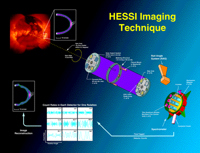
The scale of the features to be imaged with HESSI requires an angular
resolution of two arcseconds. This means being able to see
a penny at a distance of over a mile in X rays and gamma rays.
HESSI achieves this feat by using tungsten and molybdenum grids
with extremely fine slits, some as fine as 20 microns wide (less
than one thousandth of an inch). The manufacture of these
grids has been made possible by newly developed microfabrication
techniques. In addition, the mission requires the use of segmented,
hyperpure germanium detectors, with a recently developed electro-mechanical
cryocooler to maintain them at an operating temperature of minus
198 degrees Centigrade. Both developments have potential applications
in medical, industrial, and nuclear X-ray and gamma-ray imaging/spectroscopy.
Potential applications for the fine grids include X-ray imaging
for high-volume baggage inspection, characterization of heavy metal
deposits, radioactive waste assessment, and a micro mass spectrometer.
Other advanced technologies used
HESSI will make use of state-of-the-art electronic components, including advanced Field
Effect Transistors and transistor-reset Charge-Sensitive Amplifiers.


